
Copper's One-Metre Limit Is Pushing Optics Into the Package
TechCurrent Staff•11:35 UTC•13 min read
In March 2024 the IEEE P802.3dj task force adopted its objectives, the list of physical reaches the next generation of Ethernet has to survive. At 200 gigabits per second per lane, it asks a copper twinaxial cable, the shielded copper used for short direct-attach links, for a reach of up to at least 1.0 metre. It asks a single-mode fibre, at the same rate, for at least 500 metres, and separately at least 2 kilometres. At 800 Gb/s the same document adds objectives at 10 km, 20 km and 40 km. The one-metre copper figure then repeats word for word at 400G, 800G and 1.6 Tb/s.
One metre. A rack is taller than that, and a row is much longer. Once you are running 200 gigabits down a single lane, anything that has to leave the immediate neighbourhood of the chip has to become light, and the standards body wrote that down before any of this year's product announcements existed.
SEMICON Taiwan 2026 has built a large part of its programme on that gap. The show runs September 2 to 4 at the Taipei Nangang Exhibition Center, with related forums from August 31, and per Focus Taiwan was expected to draw more than 1,300 exhibitors and a record 18 national pavilions. Silicon photonics and co-packaged optics are one of the show's six technology areas, and the programme includes a Silicon Photonics Global Summit with speakers listed by EDN Asia from Cisco, Marvell, TSMC, Lumentum, ASE, UMC and Lightmatter.
40 dB at 53 gigahertz
Copper behaves the way it always did. What changed is the data rate, and a lossy electrical channel degrades badly as frequency rises.
A serial link is three things: a transmitter, a channel, and a receiver. The transmitter and receiver live in a block called a SerDes, for serializer/deserializer. When the channel is copper, the loss grows with frequency, so the faster you push the link, the more work the receiver has to do to reconstruct the bits. The 802.3dj objective for 200 Gb/s per lane over an electrical backplane tolerates a die-to-die insertion loss of up to 40 dB at 53.125 GHz. Forty decibels means the signal arriving at the far end has one ten-thousandth of the power that left. Recovering a bitstream from that requires equalisation, and past a point retiming, and both cost power that scales with the data rate. That power, which is mostly the silicon at each end fighting the cable rather than the cable itself, is what people mean by the cost of moving a bit.
The OIF's CEI-224G work, launched in early 2022, splits the electrical problem into reach classes at roughly 224 Gbps per lane:
| Class | Channel | Where it lives |
|---|---|---|
| CEI-224G-XSR | die-to-die and die-to-optical-engine | inside a co-packaged optics package |
| CEI-224G-VSR | chip-to-module | switch ASIC to a front-panel pluggable |
| CEI-224G-MR | up to 500 mm of PCB and one connector | chip-to-chip on a board |
| CEI-224G-LR | up to 1000 mm of backplane and two connectors | across a backplane |
The XSR class is worth pausing on. OIF defined a dedicated electrical interface whose only job is to carry bits the last few millimetres from a switch die to an optical engine sitting in the same package, which is not something a standards body does for a research demo.
From more than 20 dB of loss to 1 or 2
Traditionally the electrical-to-optical conversion happens in a pluggable transceiver on the front panel of a switch. Bits leave the ASIC as electrons, cross centimetres of circuit board, pass through connectors, enter a module, and only then become photons.
Mark Gardner, vice president and general manager of advanced system assembly and test at Intel, described the consequence to Semiconductor Engineering last year: "In today's pluggable optical I/O modules, the optical I/O signaling engine is outside the package of the switch/compute node. Therefore, the bottleneck of bandwidth, energy efficiency, and latency remains due to the electrical connections between the compute/switch/FPFA node and the optical engine." Co-packaging, he said, cuts the electrical signalling distance "to as low as 100µm."
In the same article, Sander Roosendaal, R&D engineering director at Synopsys Photonics Solutions, put the change in terms a SerDes designer cares about: "This reduction in electrical trace length means the SerDes (serializer/deserializer) components need to handle much lower signal loss (1 to 2 dB compared to more than 20 dB in standard designs)."
Going from more than 20 dB of channel loss to 1 or 2 dB is where most of the claimed power saving comes from. The assembly and thermal and servicing problems that come with moving optics inside the package are what that one change costs.
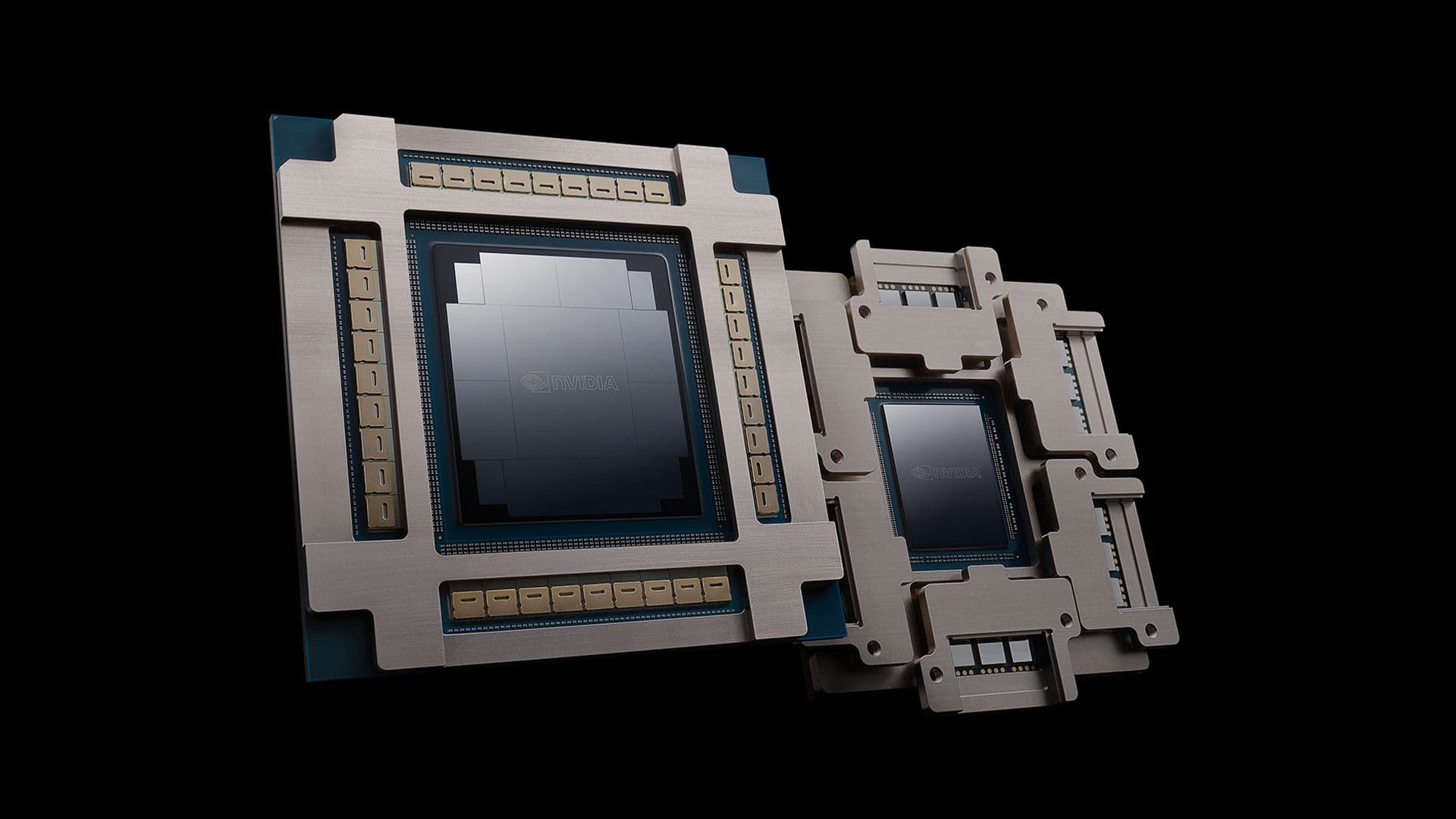
Two products are the clearest reference points. Broadcom announced Tomahawk 6 Davisson on October 8, 2025: a 102.4 Tbps Ethernet switch with 16 optical engines of 6.4 Tbps each, running 200 Gbps per link, with field-replaceable laser modules. The release describes it as supporting 512 accelerators in a scale-up domain and more than 100,000 in a two-tier network. It also says two things about status that do not sit comfortably together: that Broadcom "is now shipping" the part, and that Broadcom "is currently sampling the TH6-Davisson BCM78919 device to its early access customers and partners." Both sentences are in the same announcement.
NVIDIA's silicon photonics page lists Quantum-X InfiniBand Photonics as a current product, 144 ports of 800 Gb/s, liquid-cooled, built on 200G SerDes and with the DSP retimers removed. Spectrum-X Ethernet Photonics, up to 409.6 Tb/s, is listed as available in the second half of 2026, which as of September 3 is a stated availability window rather than a shipped product.
70% and 18% are measuring different boxes
Four sets of numbers circulate for the same technology, and they disagree because they are not measuring the same thing.
| Claim | What it measures | Source |
|---|---|---|
| 70% reduction, "more than 3.5x lower than traditional pluggable solutions" | optical interconnect power | Broadcom, Oct 8 2025 |
| 3.5x power efficiency, 4x fewer lasers, 63x better signal integrity, 10x network resiliency | CPO switches vs pluggables | NVIDIA, Mar 18 2025 |
| 5x better power efficiency, 5x sustained AI application runtime | CPO vs pluggable transceivers | NVIDIA product page, as of Sep 2026 |
| 23% vs LPO, 67% vs DSP-based | transceiver power only | Evans, *J. Lightwave Technol.* 44(16):7158-7164, 2026 |
| 44% vs LPO, 69% vs DSP-based | transceivers plus switch ASIC SerDes | same paper |
| 18% vs LPO, 36% vs DSP-based | whole switch | same paper |
Broadcom's 70% and the journal's 18% are not in conflict. One is measuring the optical interconnect subsystem; the other is measuring the box.
Alan F. Evans' 2026 paper in the Journal of Lightwave Technology walks the comparison out in stages. Counting transceivers alone, co-packaged optics comes out 23% better than linear pluggable optics and 67% better than DSP-based pluggable transceivers. Add the switch ASIC's SerDes and the gaps widen to 44% and 69%. Count total switch power, including everything that is not optics, and the reduction lands at 18% against LPO-based links and 36% against DSP-based ones. The paper indicates those gains are expected to grow.
For a power budget or a rack plan, 18 to 36% is the number to plan around. The vendor multipliers are the relevant ones if what you are comparing is optical engines. The denominators are different.
A small inconsistency inside Broadcom's own sentence is worth noting for anyone quoting it: a 70% reduction is a factor of 3.33, while "more than 3.5x lower" implies a reduction above 71.4%. Almost certainly rounding across configurations, but the two halves of that phrase are not the same claim. NVIDIA's efficiency figure also moved, from 3.5x in the March 2025 announcement to 5x on the current product page, and neither page states the comparison baseline in retrievable detail.
The per-bit figures point the same direction. ASE's April 2025 release gives 30 picojoules per bit for front-panel pluggables, 20 pJ/bit for on-board optics and under 5 pJ/bit for co-packaged optics. Vikas Gupta of GlobalFoundries told Semiconductor Engineering the move is roughly 15 pJ/bit to roughly 5, with a projected path below 1 pJ/bit. That last figure is a projection, not a measurement, and should be read as one.
Converting those into watts is straightforward arithmetic, and TechCurrent's own: a 102.4 Tbps switch moves 102.4 trillion bits a second, so at 15 pJ/bit the optical interconnect draws about 1,536 W, and at 5 pJ/bit about 512 W. Call it a kilowatt a switch. At ASE's 30 pJ/bit pluggable figure the same box would be near 3,072 W against under 512 W co-packaged. Those are order-of-magnitude conversions of published per-bit figures at full line rate, not measurements of any product, and no switch runs every lane saturated all day.
The one part that stays pluggable is the laser
Soldering the optics into the package creates a servicing problem, and the industry's answer to it went into a standard in August 2023.
OIF's External Laser Small Form Factor Pluggable implementation agreement, published August 8, 2023, defines a front-panel module that delivers continuous-wave light into a co-packaged transceiver and is "field replaceable via a pluggable electro-optic blindmate connection." The reasoning is stated plainly in the document:
"Lasers have historically demonstrated significantly lower maximum reliable junction temperatures than silicon die (including silicon photonic circuit elements and germanium photodetectors). By placing the ELSFP at the faceplate of CPO systems (removed from the heat of the co-package ASIC and OEs) a more efficient cooling solution can be designed for these systems, and greater reliability is achievable with the fail-safe of a field replaceable pluggable module in case of a laser failure."
The least reliable component in the optical chain is therefore the one part the architecture keeps replaceable, at the faceplate, well away from a die dissipating hundreds of watts. Broadcom's Davisson uses ELSFP modules. The spec also notes the form factor is designed to keep the system within IEC 60825-2 Hazard Level 1, meaning eye-safe.
ELSFP covers lasers. For everything else in the package, the industry's answer is that there is no repair path, by design. Synopsys' Roosendaal put it directly: "Instead of relying on the ability to quickly replace a failed unit with pluggable modules, co-packaged optics addresses failures by focusing on enhancing the intrinsic reliability of components and packaging, designing in redundancy, implementing integrated monitoring and self-correction." In practice that means spare lasers that can be switched in automatically when a primary one degrades, extra components built into the photonic circuits as backups, and built-in self-test. What TechCurrent could not find documented anywhere is what happens when those redundancies are exhausted, or what the field return rate looks like on deployed hardware.
A basketball-sized pipe into a pea-sized tube
The hard part of co-packaged optics is the assembly, which is why the argument is happening at a Taiwanese packaging show rather than at a networking conference.
Mitch Heins, a business development manager at Synopsys, gave Semiconductor Engineering the dimensions: a single-mode fibre core is 8 to 10 micrometres across, while a silicon-on-insulator waveguide may be 500 nanometres by 220 nanometres. He compared it to "trying to align a basketball-sized pipe to a pea-sized tube." Low-loss coupling needs alignment on the order of 0.1 µm, with traverse tolerances under 50 nm. Every detachable fibre interface costs roughly 1 dB of loss, according to GlobalFoundries' Gupta; permanent V-groove attachment loses less and cannot be repaired.
Then heat. Amkor's David Clark: "In most photonic systems, a shift in temperature of 1° C typically results in a wavelength shift of ~0.1nm." Ring resonators sitting next to a switch ASIC are being asked to hold a wavelength while the thing beside them changes temperature under load.
TSMC's remaining hurdles for volume CPO, as reported from a Silicon Photonics Industry Alliance forum in April 2026, are wafer testing, fibre array units and high-speed optical packaging assembly. TechCurrent could not retrieve that forum material directly; the detail comes via Tech Times. All three are packaging and test problems.
"In production" means four different things in Taipei
Taiwan's supply chain has spent the show announcing production status, and the phrase is doing a lot of work.
TSMC's own connectivity page, as retrieved on September 3, states that its 65nm silicon photonics technology is in volume production. The same page states that TSMC has "achieved 200 gigabits per second (Gbs) optical signal modulation and greater than 99% 3D stacking yield on engineering samples." Those are two different claims and they are worth keeping apart: a mature process node in volume, and headline performance figures demonstrated on samples. The page also says co-packaged optics "will be critical for supporting data rates of over 50 terabytes per second," and separately notes 112 Gbps SerDes IP in production.
Around the rest of the show, according to Focus Taiwan and the Taipei Times:
| Company | Reported status |
|---|---|
| TSMC | COUPE and COUPE-on-Substrate entering production in 2026 |
| UMC | first mass-produced silicon photonics wafers at its Singapore fab, with Silith Technology |
| Hon Hai (Foxconn) | expects CPO switch shipments to begin in Q3 2026 |
| ShunSin Technology | mass-production capability for 51.2 Tbps and 102.4 Tbps CPO products |
| Powertech Technology | low-volume optical engine components in 2026, full CPO switches in 2027 |
| Largan Precision | preparing trial production of an automated CPO line |
Trial production, low-volume components, mass-production capability and a volume process node are four different states of readiness. All four were described in Taipei as production. Marvell's SVP and CTO Radha Nagarajan, briefing media at the show, put silicon photonics scaling at late 2027, according to DIGITIMES (the report is paywalled beyond its headline and standfirst, so only the timeline is retrievable). TSMC's K.C. Hsu, vice president of advanced packaging technology development, told the show he expects silicon photonics to play a dominant role in 2027 with the next growth wave in 2028, per the Taipei Times.
Anything sitting on an exhibition stand is further back still. AUO Group's Daxin Materials showed a system-level Micro LED co-packaged optics module for short-reach links up to 10 metres, built with transmitters from Ennostar and receivers from Tyntek, as reported by Tech Times citing an AUO announcement TechCurrent could not retrieve directly. That is a showcase, not a shipping part.
Broadcom and NVIDIA are both selling reliability
For anyone renting capacity rather than building it, the reliability claims probably matter more than the power ones.
Broadcom's stated rationale for Davisson includes "significantly improved link flap performance and higher cluster reliability," with Near Margalit, its VP and GM for optical systems, framing the goal as "higher model FLOPs utilization, reduced job interruptions, and improved cluster reliability." NVIDIA claims 10x better network resiliency at scale and 5x sustained AI application runtime. A flapping link that kills a distributed training job costs the tenant real money in a way that a few hundred watts does not. As with cache pricing on the inference side, the number that decides the bill is not always the number on the price list. Every one of those reliability figures is a vendor claim, and TechCurrent found no independent field data on deployed CPO reliability.
TSMC's April Li, an AI and HPC business development director, told the show that data movement consumes as much as 60% of system activity in typical workloads, leaving accelerators running below 40% utilisation, and that global inference token volume has grown roughly 500-fold since 2022. That comes from the Taipei Times' report of her presentation rather than from a published benchmark, and should be read as a vendor's framing of its own market.
SEMI's Terry Tsao, its global chief marketing officer and president for Taiwan, is quoted in the organiser's own show materials, carried identically by EDN Asia and Tech Times, saying that data movement in today's AI systems "could consume more energy than computation itself, making system architecture, not individual chip performance, the new bottleneck." TechCurrent could not retrieve SEMI's own release directly, and the hedge in the quote is the organiser's own: could, not does.
Copper keeps the short links
Optics is not replacing copper. IEEE's objectives still ask for copper twinax at 200 Gb/s per lane, and OIF still defines a metre of backplane channel at 224 Gbps. Short electrical links inside a rack remain the cheapest way to move a bit and will stay that way. What keeps shrinking is the crossover distance, the point at which converting to light wins, and at 200G per lane it is down to roughly the size of a switch chassis.
Nobody in Taipei priced any of it. No vendor put a co-packaged switch up against a pluggable-based one, and none gave a dollars-per-gigabit figure, so whether CPO is cheaper at equal bandwidth is not established by anything in the public record. No shipped unit volumes either, and no independent reliability data. And for all the times COUPE has been named on stage this week, TSMC has published no datasheet for it. The company's own connectivity page does not mention COUPE at all.
“Broadcom's 70% and the journal's 18% are not in conflict. One is measuring the optical interconnect subsystem; the other is measuring the box.”
Reporting by TechCurrent Staff · TechCurrent